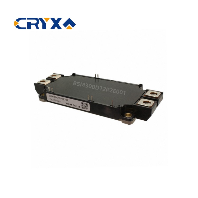
Advantages of replacing traditional MOSFETs and IGBTs with silicon carbide SIC MOSFETs
1、 11 advantages of silicon carbide mos compared to silicon mos
1. Structure and Characteristics of SiC Devices
In the Si material, the higher the voltage withstand device, the greater its on resistance per unit area (usually increased in the ratio of the voltage withstand value to the power of 2-2.5). Therefore, IGBT (insulated gate bipolar junction transistor) is mainly used for voltages above 600V. IGBT injects holes as minority carriers into the drift layer through conductivity modulation, resulting in a smaller on-resistance than MOSFETs. However, due to the accumulation of minority carriers, tail currents are generated during shutdown, resulting in significant switching losses.
http://www.ic-bom.com/The impedance of the drift layer of SiC devices is lower than that of Si devices, and it is possible to achieve high voltage withstand and low impedance using MOSFETs with high-frequency device structures without the need for conductivity modulation. Moreover, MOSFETs do not generate tail currents in principle, so using SiC MOSFETs instead of IGBTs can significantly reduce switch losses and achieve miniaturization of heat dissipation components. In addition, SiC MOSFETs can be driven under high-frequency conditions where IGBTs cannot operate, thus achieving miniaturization of passive devices. Compared with Si MOSFETs ranging from 600V to 1200V, the advantages of SiC MOSFETs lie in their small chip area (enabling small packaging) and very low recovery losses of bulk diodes.
2. Conduction resistance of SiC Mosfet
The insulation breakdown field strength of SiC is 10 times that of Si, so it can achieve high voltage resistance with a low impedance and thin drift layer. Therefore, under the same voltage withstand value, SiC can obtain devices with lower standardized on resistance (unit area on resistance). For example, at 900V, the chip size of SiC MOSFET only needs 1/35 of Si MOSFET and 1/10 of SJ MOSFET to achieve the same conduction resistance. Not only can low conduction resistance be achieved in small packages, but also the gate charge Qg and junction capacitance can be reduced. At present, SiC devices can easily achieve withstand voltage above 1700V with very low conduction resistance. Therefore, it is no longer necessary to use IGBT as a bipolar device structure (the lower the conduction resistance, the slower the switching speed), in order to achieve a device that combines various advantages such as low conduction resistance, high voltage resistance, and fast switching.
3. 3Vd Id characteristic
SiC MOSFETs, unlike IGBTs, do not have a switching voltage, so they can achieve low conduction loss in a wide current range from small to large currents. At 150 ℃, the conduction resistance of Si MOSFET increases by more than twice that at room temperature. Unlike Si MOSFET, the rise rate of SiC MOSFET is relatively low, making it easy for thermal design and having low conduction resistance at high temperatures.http://www.ic-bom.com/
4. Drive gate voltage and conduction resistance
The drift layer impedance of SiC MOSFET is lower than that of Si MOSFET, but on the other hand, according to the current technological level, the mobility of the MOS channel part of SiC MOSFET is relatively low, so the impedance of the channel part is higher than that of Si devices. Therefore, the higher the gate voltage, the lower the conduction resistance (Vgs=20V or above gradually saturates) can be obtained. If the driving voltage Vgs=10-15V used for general IGBT and Si MOSFET is used, it cannot fully utilize the low on-resistance performance of SiC. Therefore, in order to obtain sufficient low on-resistance, it is recommended to use Vgs=around 18V for driving. If Vgs=below 13V, thermal runaway may occur. Please be careful not to use it.
5. Vg-Id property
If the threshold voltage of SiC MOSFET is defined at several mA, it is equivalent to Si-MOSFET and is approximately 3V (normally closed) at room temperature. However, if a few amperes of current are flowing, the required gate voltage is about 8V or above at room temperature, so it can be considered that the resistance to false triggering is equivalent to IGBT. The higher the temperature, the lower the threshold voltage.http://www.ic-bom.com/
6. Turn On feature
The turn-on speed of SiC MOSFET is equivalent to that of Si IGBT and Si MOSFET, about tens of ns. However, in the case of inductive load switching, the recovery current generated by the return current to the upper arm diode also flows through the lower arm, resulting in significant losses due to the performance deviation of each diode. The recovery current of the bulk diodes in Si FRD and Si MOSFET is usually very high, resulting in significant losses, and this loss tends to further increase at high temperatures. On the contrary, SiC diodes are not affected by temperature and can recover quickly. Although the bulk diode of SiC MOSFET has a higher Vf, it has the same fast recovery performance as silicon carbide diodes. By quickly restoring performance through these methods, Turn-on loss (Eon) can be reduced by several tenths. The switching speed is largely determined by the external gate resistance Rg. To achieve fast action, it is recommended to use low resistance gate resistors of around a few ohms. In addition, it is also necessary to consider the surge voltage and choose a suitable gate resistor.
7. Turn Off feature
The biggest characteristic of SiC MOSFET is that it does not generate tail current, as is often seen in IGBT, in principle. Even when the voltage withstand value of SiC is above 1200V, it can adopt a fast MOSFET structure. Therefore, compared with IGBT, the Turn off loss (Eoff) can be reduced by about 90%, which is conducive to energy conservation of the circuit and simplification and miniaturization of heat dissipation equipment. Moreover, the tail current of IGBT increases with the increase of temperature, while SiC MOSFETs are almost unaffected by temperature. In addition, due to the heating caused by large switching losses, the node temperature (Tj) will exceed the rated value, so IGBTs are usually not able to be used in high-frequency areas above 20KHz. However, SiC MOSFETs can perform high-frequency switching actions above 50KHz due to their small Eoff. By high-frequency, passive devices such as filters can be miniaturized.
8. Internal gate resistance
The internal gate resistance of the chip is related to the thin layer impedance of the gate electrode material and the chip size. If it is the same design, the internal gate resistance of the chip is inversely proportional to the chip size. The smaller the chip size, the greater the gate resistance. The chip size of SiC MOSFETs is smaller than that of Si devices. Although the junction capacitance is smaller, the gate resistance is also larger.http://www.ic-bom.com/
9. Gate drive circuit
SiC MOSFET is a normally closed, voltage driven switching device that is easy to drive and has low driving power. The basic driving method is the same as IGBT and Si MOSFET. The recommended driving gate voltage is around+18V on the ON side and 0V on the OFF side. In situations where high anti-interference and fast switching are required, a negative voltage of around -3-5 V can also be applied. When driving high current devices and power modules, it is recommended to use buffer circuits.
10. Vf and reverse conduction of body diodes
Like Si MOSFETs, SiC MOSFETs also have bulk diodes (parasitic diodes) formed due to PN junctions within their bodies. However, due to the bandgap of SiC being three times that of Si, the turn-on voltage of the PN diode of SiC MOSFET is about 3V, which is relatively high, and the forward voltage drop (Vf) is also relatively high. In the past, when using fast diodes for external backflow in Si MOSFETs, due to the equal Vf size of the body diode and the external diode, in order to prevent backflow towards the slow recovery body diode side, it was necessary to connect low voltage blocking diodes in series on the MOSFET. This not only increased the number of devices, but also further worsened the conduction loss. However, the Vf of the body diode of SiC MOSFET is much higher than that of the fast diode used for reflux, so there is no need to connect the low-voltage blocking diode in series when reverse parallel connecting the external diode.
The Vf of the body diode is relatively high, which can be reduced by inputting a conduction signal to the gate electrode like rectification to reverse it. During inverter drive, the arm on the return side mostly inputs a gate conduction signal after the dead time (please confirm the action of the CPU in use). The energization of the body diode only occurs during the dead time period, and then it basically flows in the opposite direction through the channel. Therefore, even in bridge circuits composed solely of MOSFETs (SBDs without reverse parallel connection), there is no problem with the high Vf of the bulk diode.
11. Recovery characteristics of bulk diodes
Although the body diode of SiC MOSFET is a PN diode, the minority carrier lifetime is relatively short, so there is basically no accumulation effect of minority carriers. Like SBD, it has ultra fast recovery performance (tens of ns). Therefore, compared with the FRD external to IGBT, the recovery loss of Si MOSFET body diodes can be reduced to a few to tens of times that of the FRD external to IGBT. The recovery time of the body diode is the same as that of SBD, which is constant and not affected by the forward input current If (when dI/dt is constant). In inverter applications, even if only MOSFETs are used to form a bridge circuit, very small recovery losses can be achieved, and it is also expected to reduce the noise generated by the recovery current, achieving noise reduction.
From the above aspects, it can be seen that SiC MOSFETs have advantages over Si IGBTs and MOSFETs.
2、 Technical difficulties of silicon carbide moshttp://www.ic-bom.com/
Based on various reports, the challenge lies not in the principle design of the chip, especially in the structural design of the chip, which is not difficult to solve. The difficulty lies in implementing the manufacturing process of chip structure. Of course, the most direct reason for users is that the price of SiC MOSFETs is relatively high.
